Nvidia GH100 Hopper datacenter GPU specifications leaked
Some great innovations coming for GPUs
Share this article...
WePC is reader-supported. When you buy through links on our site, we may earn an affiliate commission. Prices subject to change. Learn more
A leak compilation from Videocardz and Twitter user Locuza provides an image for the GH100 block diagram and specification. Although not directly related to consumer-grade graphics cards, it’s not unusual for Nvidia to use datacenter cards as prerelease for an upcoming series. Like the Ampere A100 card came 4 months ahead of the RTX 30 series, the new Hopper cards may come a few months ahead of the RTX 4000 series.
The new Hopper datacenter accelerator is meant to be revealed on March 22nd at GTX during Nvidia’s keynote. So more information may be revealed on the upcoming lineup then but already leakers have provided the majority. With it being the first card to feature TSMCs 5nm process and all the data provided coming from the Nvidia hack a few weeks back.
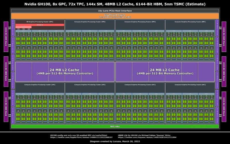
Nvidia GH100 Hopper GPU specifications
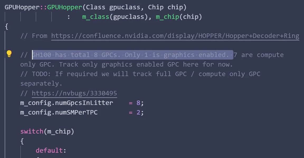
Along with the 5nm process, the datacenter accelerator only one of the graphics processing clusters (GPC) has a 3d engine, with seven lacking the feature. Clearly saving space in those clusters for other more important features used in a data center card.
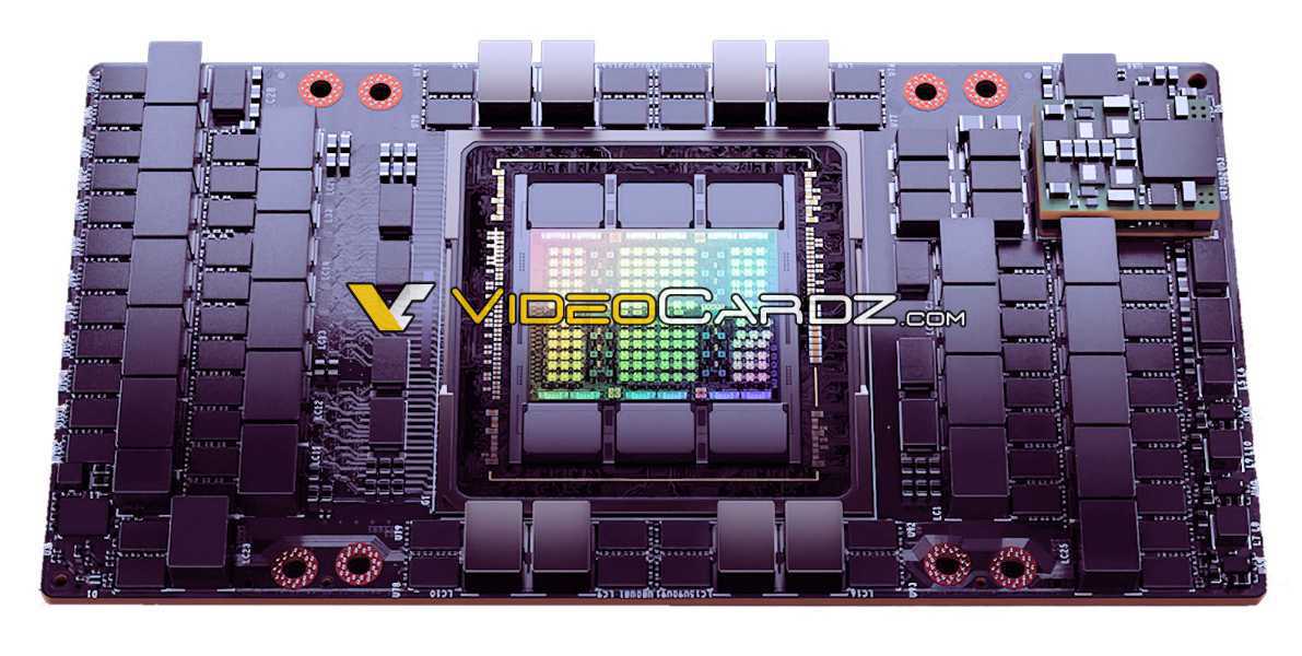
The leak also suggests the GH100 will feature 48MB of L2 cache. This isn’t a significant increase over the last generation that had 40MB but much greater than what AMD has to offer with their Aldebaran processors. It also tells us that the card will feature 8 GPCs and each cluster containing nine texture processing clusters (TPCs) which in turn have two streaming processors each.
The GH100 is also a single chip monolithic design compared to the rumored GH202 MCM design that may feature two of these GH100 dies. And bringing a similar design to wheat AMD offers in the Radeon Instinct datacenter MI250 card.
| Nvidia H100 | Nvidia A100 | Radeon Instinct MI250 | |
|---|---|---|---|
| GPU | GH100 | GA100 | Aldebaran |
| Architecture | Hopper | Ampere | CDNA2.0 |
| Foundry process | TSMC 5nm | TSMC 7nm | TSMC 6 nm |
| Transistors | ~140 billion | 54.2 billion | 58.2 billion |
| Die size | ~858+ mm2 | 828 mm2 | ~790mm2 (x2) |
| L2 cache | 48 MB | 40 MB | 16 MB |
| Memory bus | 6144-bit | 5120-bit | 8192-bit |
| Memory size | 128GB HBM3 | 40/80GB HBM2e | 128 GB HBM2e |
| TDP | 250-500W | 250-400W | 500W |
| Interface | SXM4/PCIe | SXM3/PCIe | PCIe 4.0 x16 |
| Launch year | 2022 | 2020 | 2021 |
GH100 board pictured
Videocardz has also shown what the monolithic 5nm chip will look like. The board is fitted with plenty of memory chips and a large die.