Samsung begins DDR5 memory production on a mass scale: 14nm EUV Node, 768GB capacity, 7200Mbps speeds
Samsung announce industry's smallest 14nm DRAM based on EUV technology
Share this article...

WePC is reader-supported. When you buy through links on our site, we may earn an affiliate commission. Prices subject to change. Learn more
Samsung recently announced the start of next-generation DDR5 memory production this week, all of which will be made on the company’s 14nm EUV process node. The first DDR5 arrivals will be aimed at HPC & AI servers, offering up double the performance of previous-gen DDR4 memory.
According to an official Samsung blog post, the new process node will help Samsung’s 14nm DDR5 memory achieve the highest levels of performance to date. Overall speeds will far exceed that of DDR4, with entry-level kits running at close to 4800MHz. At present, the 14nm EUV process will for speeds north of 7.2 Gbps – more than twice that of today’s DDR4 (3.2 Gbps).
Samsung state that it will be expanding its 14nm DDR5 memory portfolio to data centers, supercomputers, and enterprise server applications, allowing for even denser options based on 24Gb DRAM ICs. This would effectively allow the company to upscale their DDR5 memory from 512GB – 1TB capacities to 768GB and 1.5TB respectively.
Samsung claim industry’s smallest 14nm DRAM based on EUV technology
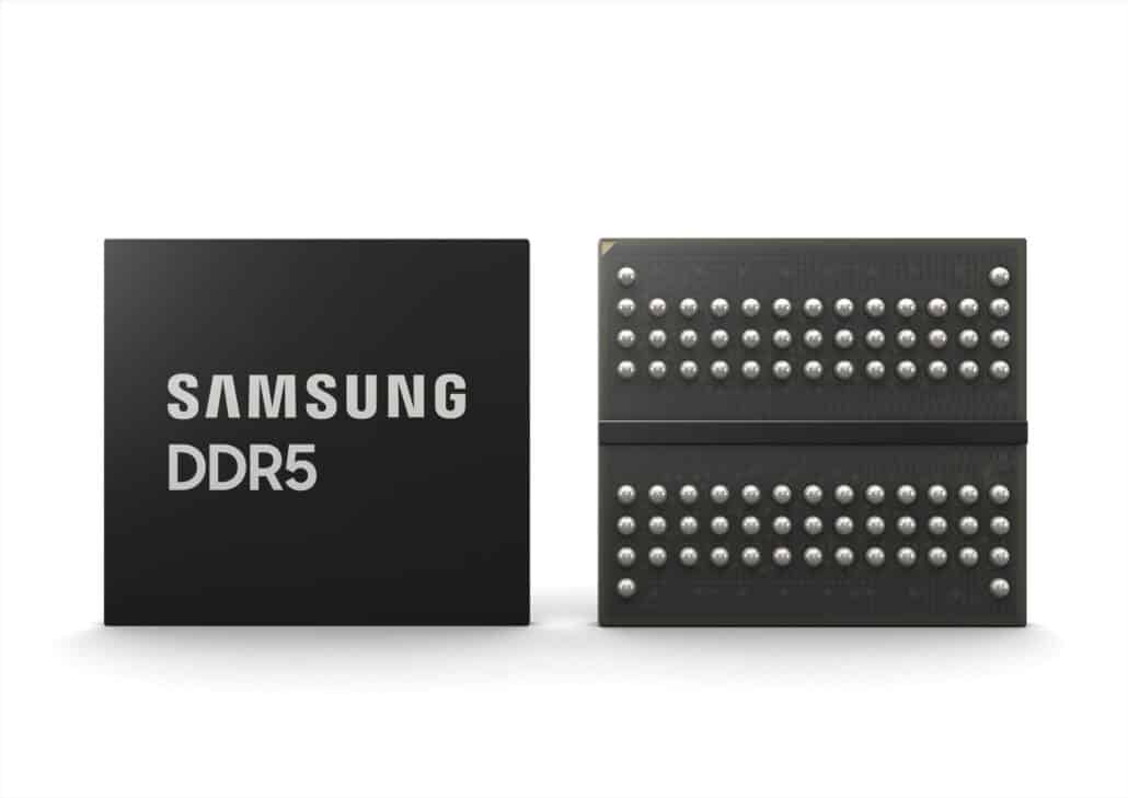
The announcement marks the production of the industry’s smallest 14nm (nanometer) DRAM based on extreme ultraviolet (EUV) technology. After the release of the company’s first EUV DRAM back in March of last year, Samsung has increased the number of EUV layers to five to help delivery the most advanced DRAM process for its DDR5 modules.
Samsung’s official post lays claim to facts such as; “Samsung’s new five-layer EUV process enables the industry’s highest DRAM bit density, enhancing productivity by approximately 20%” and “Based on the latest DDR5 standard, Samsung’s 14nm DRAM will be ideal for handling ever-growing AI and 5G workloads”.
The post continues with the following;
“We have led the DRAM market for nearly three decades by pioneering key patterning technology innovations,” said Jooyoung Lee, Senior Vice President and Head of DRAM Product & Technology at Samsung Electronics. “Today, Samsung is setting another technology milestone with multi-layer EUV that has enabled extreme miniaturization at 14nm — a feat not possible with the conventional argon fluoride (ArF) process. Building on this advancement, we will continue to provide the most differentiated memory solutions by fully addressing the need for greater performance and capacity in the data-driven world of 5G, AI, and the metaverse.“
While it may still be some time before we see DDR5 memory modules on our shelves, this is one sure step in the right direction. With DRAM now continuing to scale down to 10nm, EUV technology also becomes increasingly important in order to increase patterning accuracy. Samsung’s new EUV layering for its 14nm DRAM has helped the company achieve the highest bit density on the market – all while enhancing the overall wafer productivity by around 20%.