What does Nvidias Hopper release tell us about Lovelace?
What does all the innovation mean for the consumer?
Share this article...
WePC is reader-supported. When you buy through links on our site, we may earn an affiliate commission. Prices subject to change. Learn more
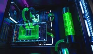
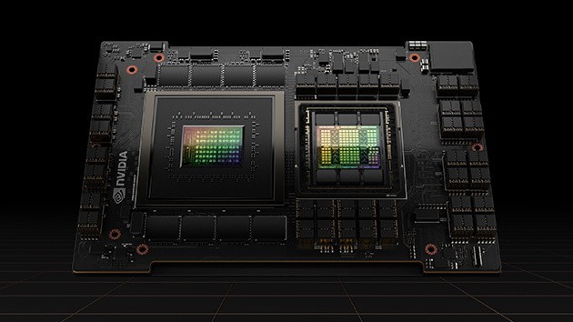
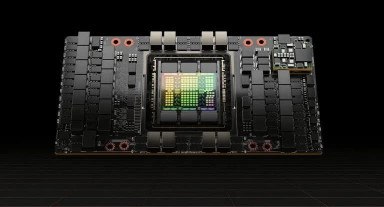
Nvidia’s newest GTC talk may not be of interest to the casual gamer but it does provide some look into the upcoming RTX 4000 series. During the presentation, they announced the GH100 Hopper datacenter GPU. Even though the card itself may not be on the radar for us it’s the architecture of the card that is the key take away.
Along with the build of the card, it is meant to be on the way during the third quarter of 2022. Which is also the likely release time for the Lovelace graphics cards. So whatever the H100 has to offer is what they’re likely to include for the consumer-grade cards. The key differences come from no MCM, maximum TDP, and fabrication node.
Lovelace fabrication node
Moore’s Law is Dead talks through what Hopper hints that Lovelace is likely to be made up. Along with his leak sources, he says that without the announcement of an MCM (Multi-Chip Module) GPU Lovelace is unlikely to be one either. AMD’s Aldebaran cards have already been out since November 2021 that feature two dies on one so you’d expect Nvidia to try to follow suit. However, with no news on MCM datacenter chips, Lovelace is unlikely to be the same as the new Radeon cards are expected to be.
However, the GH100 is made up of TSMCs 4nm process, unlike the 5nm one that was leaked beforehand. If Nvidia bought enough reservations after using Samsung in the 30 series it is possible they could use the same fabrication in the 40 series. This could be due to Nvidia trying to grab back some advantage over AMD’s MCM design and being able to fit more onto the chip.
Die size and TDP
The H100 GPU is a massive die, similar to the previous datacenter dies. It measures 814mm2 which means with its small process it can fit 80 billion transistors into it. So if Lovelace utilizes that same process it can overtake AMD in compactness since it is meant to be using a 5nm process.
GH100 also informs us of the likely max TDP the new series of cards will likely have. The highest rating it offers is 700W and datacenter cards are the top range of what a card will handle. Especially since cooling anymore is very difficult and unlikely so Lovelace is unlikely to go above that specification.